
 Yahoo Finance
RoodMicrotec uses Jenoptik’s UFO Probe® Card technology for its PIC wafer level testing
Jenoptik-UFO-Probe-Card_8635@Gnausch_300dpi_cymk

Plug & Play: the hybrid probe card UFO Probe® Card can be integrated into existing standard IC wafer probers without much effort. Picture made by Tobias Gnausch, Jenoptik.
Ufo-Probe-02
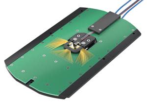
UFO Probe® Card by Jenoptik enables the parallel testing of electrical and optical components with only one probe card. Rendering made by STEP-ANI-MOTION, Jenoptik owns the complete copyright.
Wafer level testing is an important part of the supply chain of electronic components. For integrated circuits (ICs), these tests are firmly established - for photonic integrated circuits (PICs), the test ecosystem is still under development. Jenoptik provides an essential component for novel PIC wafer level tests with the opto-electronic UFO Probe® Card. RoodMicrotec benefits from a fast and simple integration, high flexibility, and state-of-the-art test technology.
Deventer, November 04, 2021 – In line with an increasing demand for photonic solutions in the semiconductor sector, the requirements for corresponding ecosystems for opto-electronic components are rising and thus, not only semiconductor manufacturers with their own supply chain must change their thinking. In addition to the existing test infrastructure for electrical components, also infrastructures for photonic component testing are required. Test houses offering services such as wafer level testing for fabless manufacturers face the challenge of expanding or reimagine their test solutions towards photonic integrated circuits (PICs).
In addition to the established tests for ICs, RoodMicrotec now also offers a test service for this new type of PIC testing at wafer level to customers from the semiconductor industry. Jenoptik provides the necessary technology platform with the UFO Probe® Card and thus supports RoodMicrotec in setting up the respective test structure.
The UFO Probe® Card from Jenoptik enables the testing of electrical and optical components with only one probe card - in parallel, not sequentially as with previous solutions. Thus, wafer level tests can be performed in a more timesaving manner and the throughput is significantly increased. As a Plug & Play solution, the hybrid probe card can be integrated directly and without much of an adaption effort into RoodMicrotec’s existing standard IC wafer probers. The existing infrastructure can be used immediately, thus simplifying the conversion of test procedures from the classic probe card for electrical components to the hybrid UFO Probe® Card within the manufacturing process.
The UFO Probe® Card does not require active alignment of the optical interfaces for every single chip. This reduces the test time and cost for each chip and thanks to the UFO Probe® Card technology, several chips can also be tested in parallel. Thus, the time needed to separate good from bad components is considerably lower if already done during PIC wafer level testing and the overall yield can be significantly improved, since only functioning chips are transferred to further manufacturing processes. Customers benefit from fewer rejects and thus reduced costs.
"As an innovative technology platform, the UFO Probe® Card offers the necessary flexibility and scalability. This enables test service providers like us to respond quickly and easily to new challenges in the market," says Jan de Koning Gans, Managing Director of RoodMicrotec GmbH.
"We are pleased to have RoodMicrotec as a strong and experienced partner for test services, and as a supply chain specialist and service provider for the semiconductor industry it also has access to a wide range of applications. It is important for Jenoptik to recognize the different needs of the end customers in order to promote relevant further developments at an early stage," says Tobias Gnausch, Product Manager for the UFO Probe® Card in Jenoptik's Light & Optics Division.
For the future, both companies plan to create standardizations for wafer level PIC testing to become even more efficient and cost-effective. With the jointly created solutions, our customers can take the step towards the future and increasingly rely on photonic solutions.
About Jenoptik and the Division Light & Optics
Optical technologies are the basis of our business: Jenoptik is a globally operating technology group and active in the three photonics-based divisions Light & Optics, Light & Production and Light & Safety. Under the brand TRIOTIPCS, Jenoptik also offers optical measurement and manufacturing systems for the quality control of lenses, objectives and camera modules. The mechatronic business is pooled under the VINCORION brand. Our key markets primarily include the semiconductor industry, medical technology, automotive and mechanical engineering, traffic, aviation as well as the security and defense technology. Worldwide, around 4,400 employees work for Jenoptik. The Group's headquarters is located in Jena (Germany). JENOPTIK AG is listed on the German Stock Exchange in Frankfurt and also on the SDax and TecDax. In the financial year 2020, Jenoptik generated sales of around 767 million euros.
Jenoptik’s division Light & Optics is a globally active OEM supplier of system solutions and products based on photonic technologies. In this, the company combines comprehensive expertise in the fields of optics, laser technology, digital imaging, optoelectronics and software. Under the brand TRIOPTICS, Jenoptik offers optical measurement and manufacturing systems for the quality control of lenses, objectives and camera modules.
Customers of the division Light & Optics include leading plant and machine manufacturers as well as equipment manufacturers in areas such as semiconductors, laser material processing, medical technology and life science, industrial automation, automotive & mobility, security and also scientific institutes.
The systems, modules and components used there help customers to optimally master their future challenges with the help of optical and photonic technologies.
Contact
Enrico Piechotka Tamara Whittaker
Global Product Group Manager Communications
JENOPTIK I Light & Optics JENOPTIK I North America
Phone: +49 3641 65-2441 Phone: +1 561 881-7400
Email: enrico.piechotka@jenoptik.com Email: tamara.whittaker@jenoptik.com
www.jenoptik.com
High resolution image is available to download from the Jenoptik image database.
You are receiving this email because you are deposited as a media representative in our files and we use this channel to keep you up to date with information from the Jenoptik Group.
In connection with the EU’s General Data Protection Regulation (GDPR), we have created a privacy policy for our currently used press distribution list. Information on the processing of personal data and your rights can be found online on our website in the Press section.
We hope that we may continue to inform you about news from the Jenoptik Group. If you do not wish to receive press releases in the future, you can unsubscribe at any time. To do so, please send a corresponding information to pr@jenoptik.com.
About RoodMicrotec
RoodMicrotec is a leading independent company for semiconductor supply and quality services. With more than 50 years of experience in the semiconductor and electronics industry, RoodMicrotec is well established as a highly valued partner for many companies worldwide. The Company provides full-turnkey ASIC services for complex microchips that are customized to handle specific applications for individual customers. In cooperation with strong partners, RoodMicrotec manages the entire development and production flow of ASICs in the target volume, ranging from low quantities up to multiple millions per year. The turnkey solution includes project management, wafer test, assembly, final test, qualification, failure analysis and logistics. All services comply with the industrial and quality requirements of the high reliability, aerospace, automotive, healthcare and industrial sectors. RoodMicrotec’s headquarters are located in Deventer, Netherlands, with operational units in Nördlingen and Stuttgart, Germany.
For more information visit https://www.roodmicrotec.com
Contact
Jan de Koning Gans
MD – Sales & Marketing
RoodMicrotec GmbH
Telefon: +49 711 86709 44
E-Mail: Jan.deKoningGans@roodmicrotec.com
www.roodmicrotec.com
This press release is published in English and German. In case of conflict between these versions, the English version shall prevail.
Attachments

